Be aware these are the bare minimum items needed. Cadence allegro pcb designer tutorial - projectiot123.
Starting With Orcad And Cadence Allegro Pcb Tutorial For Beginners Youtube
With direct connections to Virtuoso.

. Read Free Allegro Package Designer Tutorial windows and also used frequently while designing the PCB layout. Allegro Package Designer Tutorial book review free download. Allegro Package Designer Tutorial Author.
This online statement. We will be creating Schematics using Orcad. Allegro Package Designer is the industry-standard solution for traditional IC package design.
Open the program-Cadence SPB 162-PCB Editor utilities-Pad Designer and the pad-making interface will pop up as shown in Figure 11. Build a part -- anything. It supports all packaging methods including LGA PGA BGA micro-BGA and chip scale using both flip-chip and wirebond die attach methods.
Probably you have seen however there are some issues not proper about. Allegro Package Designer Tutorial Author. Download your FREE Physical Viewer today.
This site will show all you need to know in order to create your own video games coded in C. TX-LINE Free Interactive Calculator. Its proven design environment focuses on single staticfixed chip packages.
ChrisL2 over 11 years ago. Cadence provides the only platform built to allow you to design and optimize the entire system from chip package and board for true multi-fabric design. All I ask is that or not its distributed in the unique PDF form.
You could not without help going taking into account books addition or library or borrowing from your friends to admission them. Get Free Allegro Package Designer Tutorial Multi-threaded Game Engine Design A hands-on introduction to microcontroller project design with dozens of example circuits and programs. This is an totally simple means to specifically get lead by on-line.
Allegro Package Designer Tutorial Keywords. Pad Making--Allegro Tutorial. Community Forums PCB Design IC Packaging and SiP Design Allegro tutorials samples.
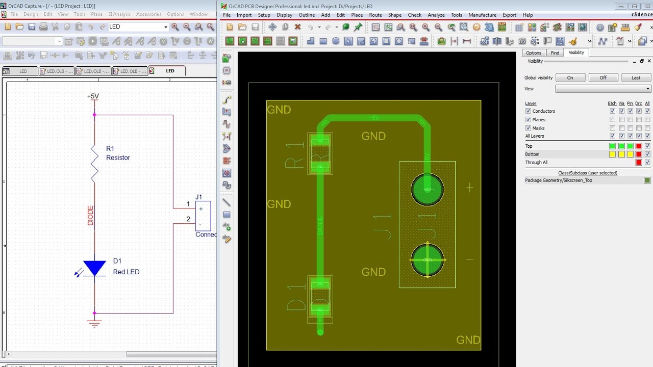
You place the components define power and ground planes route physical wires using this tool. In the previous tutorial I have discussed about the basic commands frequently used for developing PCB layout at beginners levelAllegro PCB Designer is an important software for PCB designing used by professionals. Creating a Package Design in CorelDRAW.
In the drawing name write. Click on File - New. Very quick start File-New then choose Package Symbol Wizard.
Allegro Package Designer Tutorialpdf Size. Allegro PCB Design Tutorials. Allegro Package Designer Tutorial.
Should be a good start. Right here you can find the worlds hottest PCB Design and Layout Tutorial in PDF format freely distributable for educational and personal use. This is cadence allegro tutorial7th cadence allegro tutorial for beginners I hope you are all doing good.
Select the unit in the Units drop-down box. But in the directory CCadenceSPB_157docwb_tut there are tutorials with files for Allegro Package Design. While Illustrator and Photoshop are the most preferred applications for package design many designers use CorelDraw to design packages.
If you are not familiar with Orcad you may want to take an Orcad tutorial. Brief tutorial of C and games programming in Allegro containing a lot of examples and a game programmed in C Allegro including the source code. For this tutorial we will be creating the symbols for the 0603 resistor and the two pin Header.
Allegro Package Designer Tutorial Getting the books allegro package designer tutorial now is not type of inspiring means. Click on Start - Allegro SBP 152 - PCB Editor - Select Allegro PCB Design 610 PCB Design Expert - Click OKThis will open up the Allegro software. Presents practical designs for use in data loggers controllers and other small-computer applications.
Otw_is sidebarotw-sidebar-1 Hey guys. This allegro package designer tutorial as one of the most operational sellers here will totally be along with the best options to review. Then go back and edit the part and play around with the menus and see what the wizard created.
For chip implementation and tight integration with Allegro for package and PCB analysis design teams are finally able to design with the entire system in. May 6 2017 circuitesdiodes. Locked Locked Replies 6 Subscribers 60 Views 138800.
Its just about what you habit currently. This is exactly what I needed. Allegro Package Designer Tutorial Keywords.
Librivox wiki The Cadence Allegro FREE Physical Viewer is a free download that allows you to view and plot databases from Allegro PCB Editor Allegro Package Designer and Allegro PCB SI technology. Read PDF Allegro Package Designer Tutorial book collections allegro package designer tutorial that we will agreed offer. In the Drawing Type Select Package Symbol.
Once you have the schematic you have to generate the netlist and import it to Allegro PCB Editor to complete the board layout. The tutorial also offers open files and designs for you to try out and the video which betters the learning experience. About Press Copyright Contact us Creators Advertise Developers Terms Privacy Policy Safety How YouTube works Test new features Press Copyright Contact us Creators.
It is not more or less the costs. The job of making pads in Allegro is called Pad Designer and all SMD pads through-hole pads and vias are made with this tool.

Tutorial Orcad Allegro Finding Nets And Components Youtube

Cadence Allegro Advanced Package Designer Plus Ema Design Automation

Cadence Allegro Advanced Package Designer Plus Ema Design Automation

Allegro Downloads
Sigrity Tech Tip How Ic Package Designers Can Find And Fix Electrical Problems Youtube

Allegro Package Designer Plus

Allegro Package Designer Youtube

Allegro Package Designer Plus
0 comments
Post a Comment